- 您现在的位置:买卖IC网 > Sheet目录333 > IRS25091SPBF (International Rectifier)IC MOSFET DRIVER
�� �
�
�IRS25091SPbF�
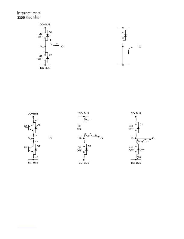
�DC+� BUS�
�Q3�
�OFF�
�V� S2�
�D3�
�I� V�
�Q4�
�ON�
�DC-� BUS�
�Figure� 14:� D3� conducting�
�Figure� 15:� Q4� conducting�
�However,� in� a� real� inverter� circuit,� the� V� S� voltage� swing� does� not� stop� at� the� level� of� the� negative� DC� bus,� rather� it� swings� below� the�
�level� of� the� negative� DC� bus.� This� undershoot� voltage� is� called� “negative� V� S� transient”.�
�The� circuit� shown� in� Figure� 16� depicts� one� leg� of� the� three� phase� inverter;� Figures� 17� and� 18� show� a� simplified� illustration� of� the�
�commutation� of� the� current� between� Q1� and� D2.� The� parasitic� inductances� in� the� power� circuit� from� the� die� bonding� to� the� PCB� tracks�
�are� lumped� together� in� L� C� and� L� E� for� each� IGBT.� When� the� high-side� switch� is� on,� V� S1� is� below� the� DC+� voltage� by� the� voltage� drops�
�associated� with� the� power� switch� and� the� parasitic� elements� of� the� circuit.� When� the� high-side� power� switch� turns� off,� the� load� current�
�momentarily� flows� in� the� low-side� freewheeling� diode� due� to� the� inductive� load� connected� to� V� S1� (the� load� is� not� shown� in� these�
�figures).� This� current� flows� from� the� DC-� bus� (which� is� connected� to� the� COM� pin� of� the� HVIC)� to� the� load� and� a� negative� voltage�
�between� V� S1� and� the� DC-� Bus� is� induced� (i.e.,� the� COM� pin� of� the� HVIC� is� at� a� higher� potential� than� the� V� S� pin).�
�Figure� 16:� Parasitic� Elements�
�Figure� 17:� V� S� positive�
�Figure� 18:� V� S� negative�
�In� a� typical� motor� drive� system,� dV/dt� is� typically� designed� to� be� in� the� range� of� 3-5� V/ns.� The� negative� V� S� transient� voltage� can�
�exceed� this� range� during� some� events� such� as� short� circuit� and� over-current� shutdown,� when� di/dt� is� greater� than� in� normal� operation.�
�International� Rectifier’s� HVICs� have� been� designed� for� the� robustness� required� in� many� of� today’s� demanding� applications.� An�
�indication� of� the� IRS25091’s� robustness� can� be� seen� in� Figure� 19,� where� there� is� represented� the� IRS25091� Safe� Operating� Area� at�
�V� BS� =15V� based� on� repetitive� negative� V� S� spikes.� A� negative� V� S� transient� voltage� falling� in� the� grey� area� (outside� SOA)� may� lead� to� IC�
�permanent� damage;� viceversa� unwanted� functional� anomalies� or� permanent� damage� to� the� IC� do� not� appear� if� negative� Vs� transients�
�fall� inside� SOA.�
�At� V� BS� =15V� in� case� of� -V� S� transients� greater� than� -16.5� V� for� a� period� of� time� greater� than� 50� ns;� the� HVIC� will� hold� by� design� the�
�high-side� outputs� in� the� off� state� for� 4.5� μ� s.�
�www.irf.com�
�11�
�发布紧急采购,3分钟左右您将得到回复。
相关PDF资料
IRS2509SPBF
IC MOSFET DRIVER
IRS26072DSPBF
IC DVR HI/LOW SIDE 600V 8-SOIC
IRS2607DSTRPBF
IC DVR MOSFET/IGBT N-CH 8-SOIC
IRS2608DSTRPBF
IC DRIVER MOSFET/IGBT 8-SOIC
IRS2609DSPBF
IC DVR MOSFET/IGBT N-CH 8-SOIC
IRS26302DJTRPBF
IC GATE DRIVER 3PH BRIDGE 44PLCC
IRS26310DJTRPBF
IC DRIVER MOSFET/IGBT 44-PLCC
IRS4427PBF
IC MOSFET DRIVER
相关代理商/技术参数
IRS25091STRPBF
功能描述:功率驱动器IC 600V 999A OTHER RoHS:否 制造商:Micrel 产品:MOSFET Gate Drivers 类型:Low Cost High or Low Side MOSFET Driver 上升时间: 下降时间: 电源电压-最大:30 V 电源电压-最小:2.75 V 电源电流: 最大功率耗散: 最大工作温度:+ 85 C 安装风格:SMD/SMT 封装 / 箱体:SOIC-8 封装:Tube
IRS2509SPBF
功能描述:功率驱动器IC Half-Bridge Driver 600V 120mA 530ns RoHS:否 制造商:Micrel 产品:MOSFET Gate Drivers 类型:Low Cost High or Low Side MOSFET Driver 上升时间: 下降时间: 电源电压-最大:30 V 电源电压-最小:2.75 V 电源电流: 最大功率耗散: 最大工作温度:+ 85 C 安装风格:SMD/SMT 封装 / 箱体:SOIC-8 封装:Tube
IRS2509STRPBF
功能描述:功率驱动器IC 600V 999A OTHER RoHS:否 制造商:Micrel 产品:MOSFET Gate Drivers 类型:Low Cost High or Low Side MOSFET Driver 上升时间: 下降时间: 电源电压-最大:30 V 电源电压-最小:2.75 V 电源电流: 最大功率耗散: 最大工作温度:+ 85 C 安装风格:SMD/SMT 封装 / 箱体:SOIC-8 封装:Tube
IRS2526DSPBF
功能描述:功率驱动器IC 600V Mini Ballast Controller Icr RoHS:否 制造商:Micrel 产品:MOSFET Gate Drivers 类型:Low Cost High or Low Side MOSFET Driver 上升时间: 下降时间: 电源电压-最大:30 V 电源电压-最小:2.75 V 电源电流: 最大功率耗散: 最大工作温度:+ 85 C 安装风格:SMD/SMT 封装 / 箱体:SOIC-8 封装:Tube
IRS2526DSTRPBF
功能描述:功率驱动器IC 600V Mini Ballast Controller Icr RoHS:否 制造商:Micrel 产品:MOSFET Gate Drivers 类型:Low Cost High or Low Side MOSFET Driver 上升时间: 下降时间: 电源电压-最大:30 V 电源电压-最小:2.75 V 电源电流: 最大功率耗散: 最大工作温度:+ 85 C 安装风格:SMD/SMT 封装 / 箱体:SOIC-8 封装:Tube
IRS2530
制造商:未知厂家 制造商全称:未知厂家 功能描述:DIMMING BALLAST CONTROL IC
IRS2530D
制造商:IRF 制造商全称:International Rectifier 功能描述:DIM8TM DIMMING BALLAST CONTROL IC
IRS2530DPBF
功能描述:功率驱动器IC Ballast Cntrl IC 600V .500A RoHS:否 制造商:Micrel 产品:MOSFET Gate Drivers 类型:Low Cost High or Low Side MOSFET Driver 上升时间: 下降时间: 电源电压-最大:30 V 电源电压-最小:2.75 V 电源电流: 最大功率耗散: 最大工作温度:+ 85 C 安装风格:SMD/SMT 封装 / 箱体:SOIC-8 封装:Tube